RAM-Based State Machine
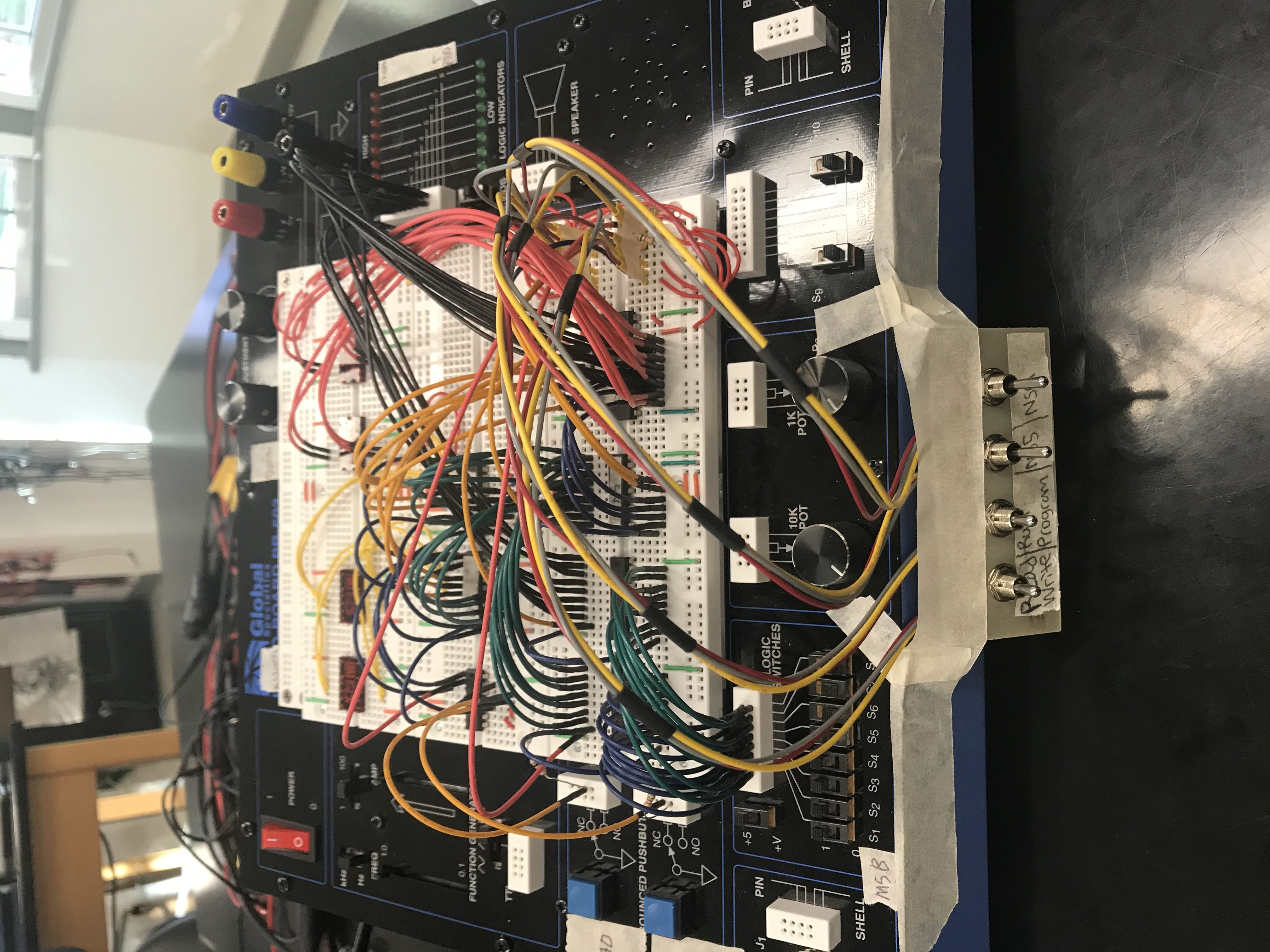
For one of the final lab assignments of my analog and digital electronics course, we made a RAM-based state machine. It could read/write programs to a “static RAM’ memory IC. We used it to enter a pre-written program with a secret message to memory. Our task was to decode the message by running the program and viewing the code on the hexadecimal displays. The message read “DECAF COFFEE”. There are three main parts to the machine: an 8-bit counter, 3-state buffer, and static RAM circuit.
Lab Description
We used the NTE6810 memory chip which has 128 locations, each of which can store a byte. Note that 128 locations require 7 bits of address information. The data pins are bi-directional and 3-state. If the R/W pin is HIGH, then the memory chip is in READ mode and the data pins are outputs. If the R/W pin is LOW, then the data pins are inputs. The address pins are always inputs. A 3-state (sometimes called tri-state) output can be in a logic LOW state, logic HIGH state, and a high-impedance state which is neither HIGH nor LOW. In this state, another device can take over and drive the line connected to the disabled output to a valid logic state. We used the 74HC541 chip, which has 3-state outputs, to create an octal buffer with an 8-bit DATA IN buss and 8-bit DATA OUT buss.
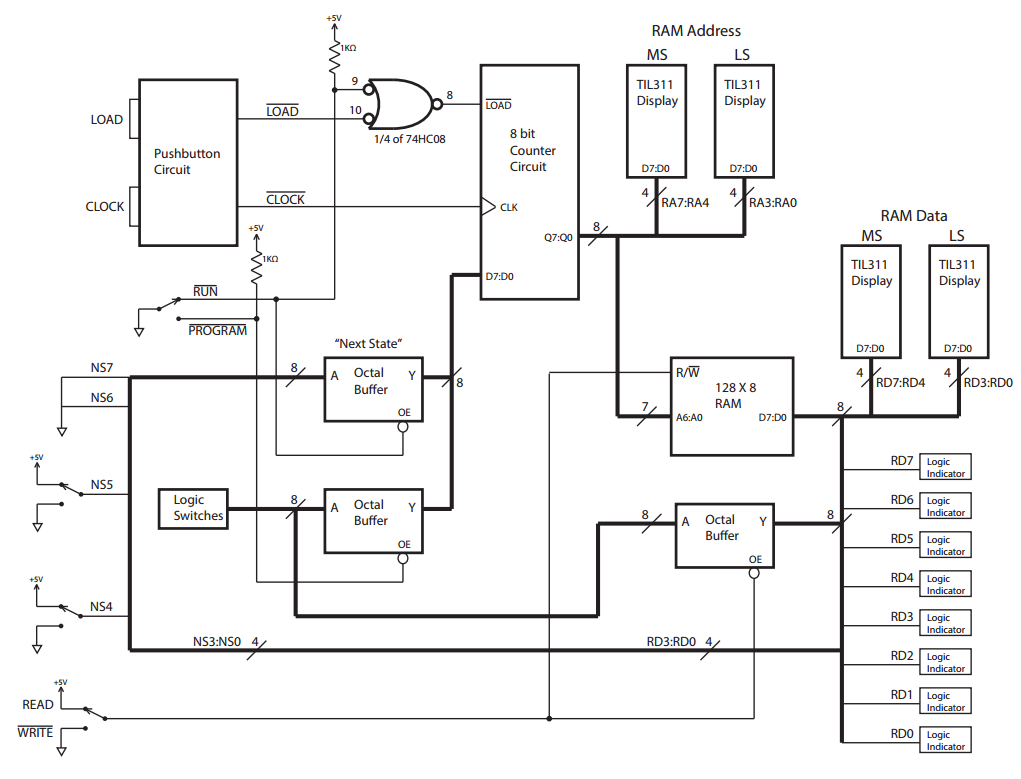
The 8-bit counter was constructed using two 74LS569 ICs, a pushbutton circuit, set of logic switches, and two TIL311 displays. Pushing the LOAD button in the pushbutton circuit loads the binary value set by the logic switches into the counter, and pushing the CLOCK button increments the counter from that point.
The 8-bit counter generates the 7-bit addresses for the RAM (with one bit left over). When programming the RAM, the logic switches are used to load data into the address counter and into the RAM. Four TIL311 displays show the RAM address and RAM data. When the state machine is running, the four lowest RAM data bits (RD3:RD0) are fed back to determine the next state (NS3:NS0). The next two bits of the next state buss (NS5:NS4) are set by switches. The highest two next state bits (NS7:NS6) are set LOW by tying them to ground.
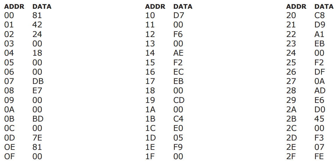
A hierarchical circuit diagram of the machine is attached in the Image Gallery. The data for three programs I entered into the machine is also included in the Image Gallery. The first program looks nice on the logic indicator LEDs; the other two programs present the secret message on the MS data hex display.
Image Gallery
 Finished Version of Machine on Protoboard
 Hierarchical Circuit Diagram of Machine
 Data for Three Machine Programs